The standard excuse for any delayed fab project is complexity: American labor rules, local permitting, supply chain friction, the sheer difficulty of transplanting semiconductor manufacturing to unfamiliar soil. TSMC used that excuse — reasonably — when Fab 21's Phase 1 ramp ran behind schedule. Now the company appears to be dismantling it.
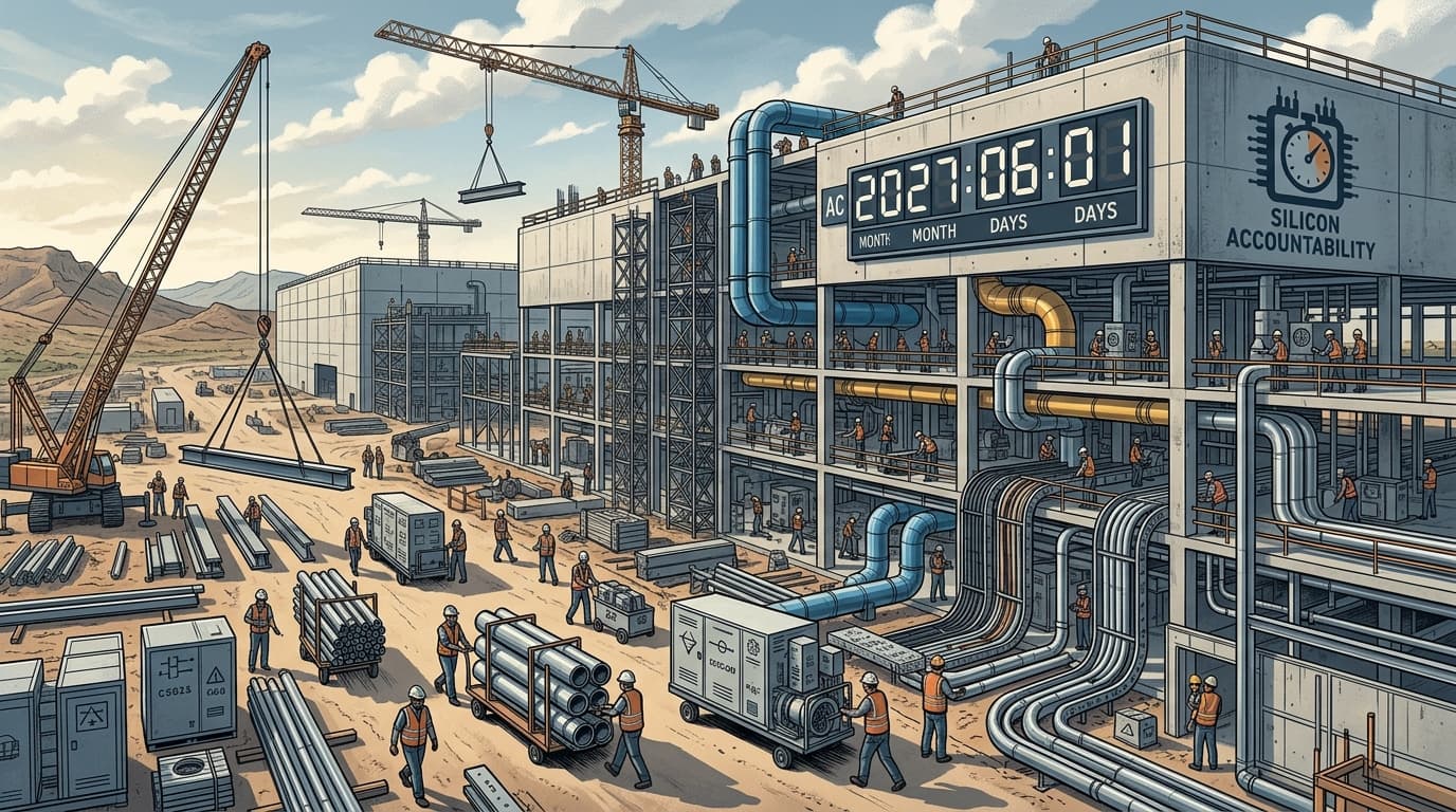
According to TrendForce, citing Commercial Times sources, TSMC has pulled forward the construction timeline for Fab 21's Phase 2 (P2) in Arizona, with 3nm mass production now targeted for the second half of 2027. More striking: the company has reportedly compressed U.S. build timelines from roughly three years for P1 to approximately 1.5 to 2 years for subsequent phases — approaching Taiwan's domestic efficiency. The mechanism is straightforward. TSMC is deploying more personnel to Arizona, specifically targeting cleanroom mechanical, electrical, and plumbing (MEP) engineering, which the report identifies as the critical bottleneck. Overseas builds that once required six quarters are now being completed in four to five.
That's a real operational improvement, not a PowerPoint revision. But "targeting second half of 2027" covers a lot of ground. Watch for equipment installation milestones at P2 over the next two quarters — those are the leading indicators that separate an accelerated schedule from an accelerated press release.
Four Fabs Booked, But the Demand Story Needs Scrutiny
The same TrendForce report states that all four of TSMC's planned U.S. fabs are "fully booked" by customers. Take that claim seriously but not literally. Fab capacity bookings at this stage typically reflect letters of intent and preliminary agreements, not binding purchase commitments with penalty clauses. The AI demand tailwind is real, and TSMC's customer concentration — Apple, NVIDIA, AMD — gives those bookings more weight than a typical foundry's order book. But "fully booked" in 2026 for fabs coming online in 2027 and beyond is a forecast dressed as a fact.
The more durable signal: TSMC is simultaneously accelerating sub-2nm equipment installation at Hsinchu Fab 20 and Kaohsiung Fab 22 in Taiwan, per the same report. A company hedging on U.S. demand would not be running parallel acceleration programs across three continents. The operational posture suggests genuine confidence in the order pipeline — even if the booking language is doing some marketing work.
The CHIPS Act's Structural Problem Hasn't Gone Away
While TSMC's Arizona execution is improving, the policy architecture funding it remains contested. A Washington Examiner op-ed drawing on Competitive Enterprise Institute analysis highlights what it calls the CHIPS Act's "fungibility problem": federal funding directed at fab construction cannot be cleanly separated from a recipient company's broader capital allocation decisions. The stock buyback restriction in Section 102(g) applies only to funds explicitly traceable to CHIPS awards — companies can use other internal funds for buybacks while CHIPS money flows into construction budgets.
This is a structural critique worth tracking, not because it invalidates the program, but because it shapes how to evaluate whether the $52 billion in direct incentives is actually changing corporate behavior or simply subsidizing investments companies would have made anyway. The honest answer is probably "both, in proportions we can't precisely measure" — which is exactly the kind of ambiguity that makes industrial policy accountability difficult.
The CHIPS Act's original strategic premise — reducing U.S. dependence on foreign fabs, which fell from 37% of global semiconductor manufacturing in 1990 to under 10% by 2022 — remains sound. The execution question is whether the funding structure was calibrated to achieve that goal or to generate announcement-friendly ribbon cuttings.
Intel's 18A: The Milestone That Actually Matters This Year
Intel's process roadmap recovery hinges on 18A, its most advanced node and the one it needs to prove foundry credibility. As of early March 2026, the company was positioning 18A as its inflection point — the node where it closes the gap with TSMC's N2 and reclaims manufacturing relevance, per FinancialContent's analysis.
The accountability question isn't whether Intel believes in 18A — of course it does. The question is yield. Process node announcements are cheap; high-volume production at competitive yields is the only metric that matters for foundry customers making tape-out decisions. Intel has a history of announcing nodes and then quietly revising what those nodes actually deliver. Watch for external customer tape-out confirmations on 18A in the second half of 2026. A named customer committing real silicon to 18A is worth more than any earnings call statement about manufacturing progress.
What to Watch in the Next 90 Days
Three concrete milestones will tell us more than the next quarter of press releases. First: TSMC P2 equipment installation progress in Arizona — any public confirmation of tool-in dates would validate the compressed timeline claim. Second: Intel's next earnings call, expected in late April, for any update on 18A customer engagements beyond the Panther Lake internal product. Third: Commerce Department disbursement data on CHIPS Act awards — the gap between announced funding and actual cash out the door remains the program's most underreported accountability metric.
The optimistic timeline is getting shorter. So is the window to verify it.


